OASIS-8C: Verilog Design and FPGA Prototyping of 8-core OASIS Network-on-Chip System
Project Goal†
- Real design in verilog HDL and prototyping on FPGA of a small scale 8-core OASIS Network-on-Chip System.
- Detailed Design Manual.
Members†
- Nam Khanh Dang
- Akihito Kajikawa
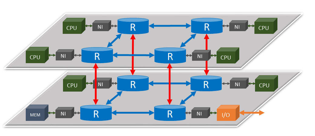
System Architecture†
Specification†
- System specifications:
- OASIS 3D Network-on-Chip [Ref.1].
- Network Interface: [Ref.2].
- Processing Elements:
- CPU: MIPS
- MEM: TBD
- I/O: TBD
- Application specifications:
- Target CPU: MIPS.
- Target applications: TBD.
- Implementation environment:
- Language: Verilog HDL.
- Simulation tool: Modelsim Altera.
- Implementation tool: Altera Quartus II.
- Implementation board: Spartan DE II.
- Resource:
- Logic:
- Register:
- I/O:
- External devices:
- Note:
Hardware Prototyping Phases†
- Step 01: Design Preparation.
- Decide the system's specification.
- Prepare the required tools, boards and source code.
- Step 02: Individual Network Tile (PE-NI-R) Implementation.
- Establish an individual network tile: PE(Processing Element) - NI(Network Interface) - R(Router).
- I/O Interface connection.
- Connection synchronization.
- Demo application implementation.
- Step 03: 2D 2x2 Network Implementation.
- Establish a 2D 2x2 Network Implementation (2 CPUs, 1 Memory, 1 I/O).
- Demo application implementation.
- Step 04: 3D 2x2x2 Network Implementation.
- Establish the proposal architecture.
- Demo application implementation.
Schedule†
| Stage | Content | Start Date | Finish Date | Note |
| 1 | Design Preparation | 2015/June/02 | 2015/June | . |
| 2 | An Individual Network Tile | TBD | TBD | . |
| 3 | A 2D Network | TBD | TBD | . |
|4|The complete system|TBD|TBD|.|
References†
Last Update:
- 2015 June 8th: Update system architecture diagram.
![[PukiWiki]](image/pukiwiki.png "[PukiWiki]")