 |
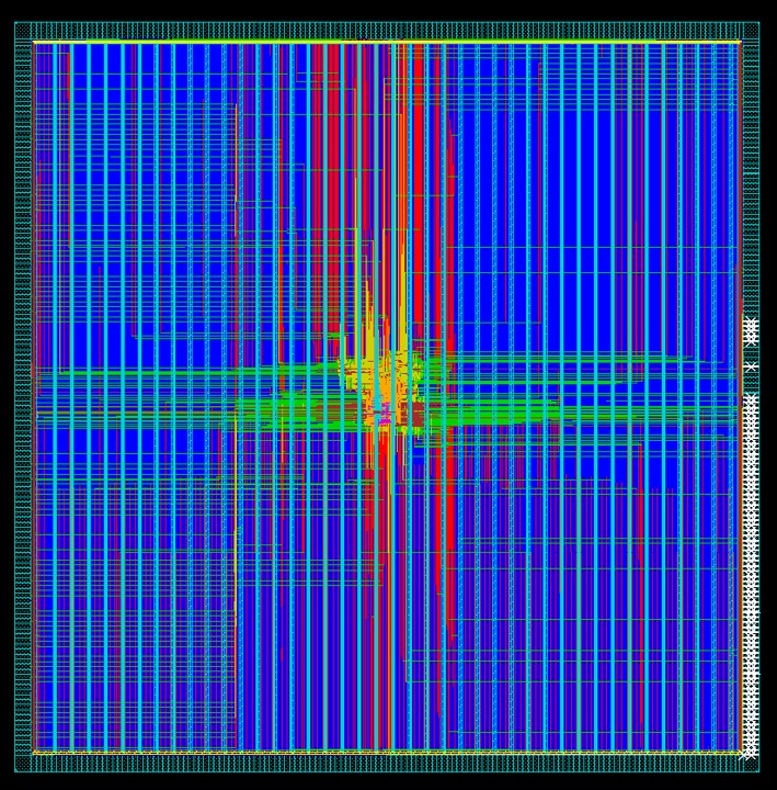
| OASIS-RV1 Chip Layout. JUly 7, 2014. |
- Technology: 45nm CMOS Process
- Chip Size: ......... Please complete this
- Function: Router for 3D NoC System
- Frequency: ........... Please complete this
- Power Dissipation: 222.387 uW
- Number of Pins: 557
- Completion Date: July 5th (expected)
OASIS 3D Router Tutorials†
1. Synthesis with Design Compiler†
2. Place & Route with SoC Encounter†
3 Design Checking: LVS (Layout-Versus-Schematic) and DRC (Design-Rule Check)†
4 Post Layout Simulation:†
5 Pad Insertion†
6. Chip Submission†
- PDF, PPT, Completion Date: July 15th
PHENIC Control Router†
This tutorial will be completed by November 10th 2014
- 1. Synthesis with Design Compiler
- 2. Place & Route with SoC Encounter
- 3 Design Checking: LVS (Layout-Versus-Schematic) and DRC (Design-Rule Check)
- 4 Post Layout Simulation:
- 5 Pad Insertion
- 6. Chip Submission
Reference: MIPS processor Tutorials†
- Complete tutorial of MIPS processor prototyping on ASIC (in Japanese),
zip file
How to Login and use VDEC tools on zxp035†
- To use VDEC tools on zxp035 machine type the following comand in your terminal
- Password : blm2011
- design_vision (to use Design Compiler)
- velocity (to use SoC Encounter)
- simvision (to use Simvision)
Registerd IPs @ with VDEC Server†
Links†
![[PukiWiki]](image/pukiwiki.png "[PukiWiki]")


